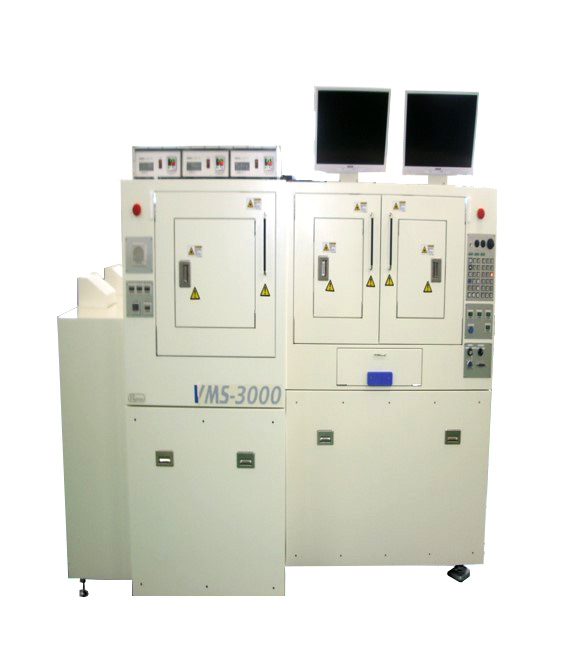
LD Chip Tester VMS3000
Laser Diode Chip Tester VMS3000
VMS3000 consists of a series of laser diode chip testers, designed to automatically pick up LD chips from tape and transfer them to temperature-controlled chucks to perform LIV, FFP and wavelength test; before sorting the chips and placing them on tape or Gel Pak according to preset criteria.
The series includes VMS3100, VMS3200 and VMS3300.
▪ VMS3100 utilize a single temperature-controlled table to test chips at 25°C.
▪ VMS3200 use two temperature-controlled tables to test chips at 25°C.and 85°C.
▪ VMS3300 use two temperature-controlled tables to test chips at 25°C and 85°C in addition to a third table to conduct top and facets visual inspection.
This high precision series of chip testing machines includes a number of design features that allows accurate, robust and consistent opto-electrical characterization and sorting. Features includes a state-of-the-art vision system, scanning functions ,Test table positioning function and No Good (NG) management function with option to leave NG chips on supply ring, place measured chips on ring ,tape, Gel Pak or in a NG box.
Features
• Designed to support R & D and production environments • Automatic chip sorting and placement function and options
• Fully automatic characterization of laser chips
• State of the art vision system
• Optical Character Recognition (OCR) for chip recognition
• Flexibility to include testing equipment or integrate customers testing equipment
• One ,Two or Three independently temperature-controlled measurement tables
• Optical output power and spectrum measurement at two different temperatures
• High Throughput due to design allowing parallel handling of multiple chips
• Flexible and Adjustable to handle laser for all applications from UV to IR
• Applicable for chips down to 150μm x 200μm lateral size & 100μm substrate thickness
Specification
1. Wafer Table • Table φ170 mm (For maximum 4 inches wafer)
• Parallel ±0.010 mm/100mm Travel
• Wafer Ring Size 6-Inch Frame 2-6-1 (Disco Standard)
2. Laser Unit
• Laser Source 355nm Nano Second Laser
• Ave. Power 5W
3. Optical Unit
• X 100 Lens for Laser
• x20 Lens for Monitor & Alignment with Auto Focusing
4.Vision System
• Camera 1 for Wafer Positioning
• Camera 2 for Alignment with Auto Focusing
5. Controller
• PLC Control
• Parameters are input through the touch screen.
• A set of parameters is saved for each model as a recipe and read
by selection.
• Maximum 20 recipes can be stored
6. Machine Body
• Laser Safety Level: Class 1 • Color: Opto Standard
7. Utilities
• Power Supply AC100V 1.2KVA
• Vacuum Vacuum Pump Supplied /Factory Line
• Air Supply 5Kg/cm2 Φ6mm
8. Size ・1200(W) × 1300(D) × 6700(H) mm
9. Weight ・ Approx. 700 Kg
10.Signal Tower ・ 3 Color status signal tour
Product Inquiry Form