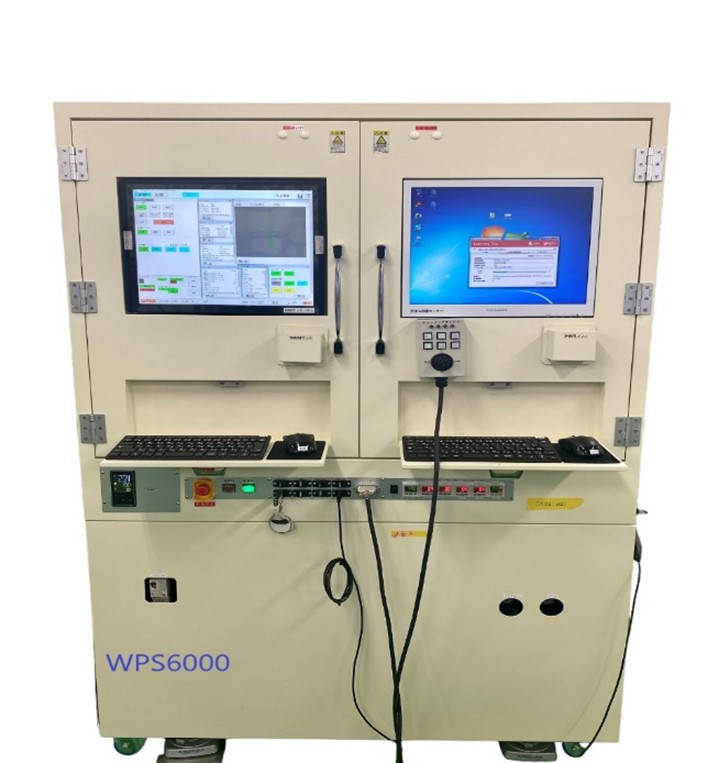
Wafer Prober WPS6000
on
• For wafer sizes of up to 6”
• Integration of testing equipment with precise alignment of chips and prober needles.
• Flexibility to include testing equipment or integrate customers testing equipment
• State of the art vision system
• High productivity , precise placement ,excellent contact performance and high-speed control
• High precision ,robust and dependable tool for high-yield mass production
• Flexible tool for R&D. Statistical big data can be acquired in minutes
• Used for Bulk Acoustic Wave (BAW) and Surface Acoustic Wave (SAW) filter probing
• Applicable for LED testing and VCSEL diode chip characterization
• TeamViewer remote access
• Target Wafer : Many kinds of chips: SAW Filters, LEDs, VCSELs…
• Wafer Size : φ6inch wafer (1/4 split wafer available)
• Wafer Thickness: 0.1 to 0.6mm
• Chip Size: 0.2 to 1.0mm
• Measurement area Ø195mm on taped frame
2. Tact Time
• Throughput: 2.5sec/chip
• Mechanical Index Time: 200msec/0.3mm
• Measurement time: 1.0sec or less
3. Machine Size: 1140(W) × 1110(D) × 1750(H) mm
4. Machine Weight: Approx. 1500 Kg
5. Utility
• Power Supply: AC 100V 50/60Hz
• Power consumption: 1.5kVA (main unit only)
• Air source: Factory line 4~7kg/cm2,
• Tube outer diameter φ8mm: Dry air (for condensation countermeasures) 4~7kg/cm2, tube outer diameter φ8mm
When using a measurement stage of 20°C or less, about MAX100L/min is required.
• Vacuum source: Vacuum pump tube outer diameter φ8mm
• Operating environment: Temperature 25°±2°, humidity 60%RH or less
Wafer Prober WPS6000
The WPS6000 Semi -Automatic Wafer Prober is designed to meet the handling and test requirements of Laser Diode (VCSEL) ,optical device (LED) and other markets including Bulk Acoustic Wave (BAW) and Surface Acoustic Wave (SAW) filter probing.
The operator manually loads the wafer on the measuring table before starting the machine to automatically conduct electrical test of each die on the wafer, to determine the overall quality and functionality of the wafer.
The WPS6000 Prober handles wafers up to 6” in diameter. The prober use probe needles to contact the chips from the top and electrically characterize all chips. If both contacts(connection pads) are on the top, the chips can remain on the tape this allows the vision system to accurately align and monitor the measurement. If one contact is on the bottom, the chips are accurately transferred to a wafer chuck to complete the electrical test.
The machine design incorporates a highly flexible and reliable platform that is able to integrate customer’s existing testing equipment or a turnkey testing system included by Opto System. WPS6000 consistently achieve high productivity , precise placement ,excellent contact performance and high-speed control. This machine is suitable for both R&D and mass production and is popular with our customers worldwide to meet the handling and test requirements of Laser Diode (VCSEL) ,optical device (LED) and other markets including Bulk Acoustic Wave (BAW) and Surface Acoustic Wave (SAW) filter probing.
Features
• Fully automatic electrical testing and characterization of chips on tape• For wafer sizes of up to 6”
• Integration of testing equipment with precise alignment of chips and prober needles.
• Flexibility to include testing equipment or integrate customers testing equipment
• State of the art vision system
• High productivity , precise placement ,excellent contact performance and high-speed control
• High precision ,robust and dependable tool for high-yield mass production
• Flexible tool for R&D. Statistical big data can be acquired in minutes
• Used for Bulk Acoustic Wave (BAW) and Surface Acoustic Wave (SAW) filter probing
• Applicable for LED testing and VCSEL diode chip characterization
• TeamViewer remote access
Specification
1. Target Wafer• Target Wafer : Many kinds of chips: SAW Filters, LEDs, VCSELs…
• Wafer Size : φ6inch wafer (1/4 split wafer available)
• Wafer Thickness: 0.1 to 0.6mm
• Chip Size: 0.2 to 1.0mm
• Measurement area Ø195mm on taped frame
2. Tact Time
• Throughput: 2.5sec/chip
• Mechanical Index Time: 200msec/0.3mm
• Measurement time: 1.0sec or less
3. Machine Size: 1140(W) × 1110(D) × 1750(H) mm
4. Machine Weight: Approx. 1500 Kg
5. Utility
• Power Supply: AC 100V 50/60Hz
• Power consumption: 1.5kVA (main unit only)
• Air source: Factory line 4~7kg/cm2,
• Tube outer diameter φ8mm: Dry air (for condensation countermeasures) 4~7kg/cm2, tube outer diameter φ8mm
When using a measurement stage of 20°C or less, about MAX100L/min is required.
• Vacuum source: Vacuum pump tube outer diameter φ8mm
• Operating environment: Temperature 25°±2°, humidity 60%RH or less
Product Inquiry Form